|
Department of Electrical and Computer Engineering Microelectronic Circuit Design Group |
|
Department of Electrical and Computer Engineering Microelectronic Circuit Design Group |
Benchmark Evaluation of MOSFET Models (BEMOS) is a program developed in the Cadence programming language (SKILL).
It requires Cadence release 5.1.41 or newer to properly run. It is independent of the operating system environment,
meaning that it works in every OS that Cadence supports (HP-UX, Solaris, Linux).
BEMOS is used to easily perform benchmark tests on MOS models. It supports both NMOS and PMOS models written for the
Spectre simulator. It also supports MOS devices build as a subcircuit structure.
System Requirements: Cadence release 5.1.41.
If you are interested in a free copy of the program or if you have any questions please send an e-mail to
bemos@elab.ntua.gr.
If you would like a copy of BEMOS, please, fill in this form
and include it as an attachment in the e-mail.
Currently supported are the following IEEE recommended tests (more information available here):
1.
I-V characteristics
A.
Playbacks of Id
and gd versus Vds in saturation region, for wide/long and wide/short
devices. The playbacks are for Vsb=0
and Vsb=Vdd, Vgs=Vth-0.15,
Vth, Vth+0.15,
and 3 values of Vgs equally spaced between Vth and Vdd,
and Vds swept from 0 to Vdd
in 0.02 V steps.
B.
Playbacks of Id
and gm versus
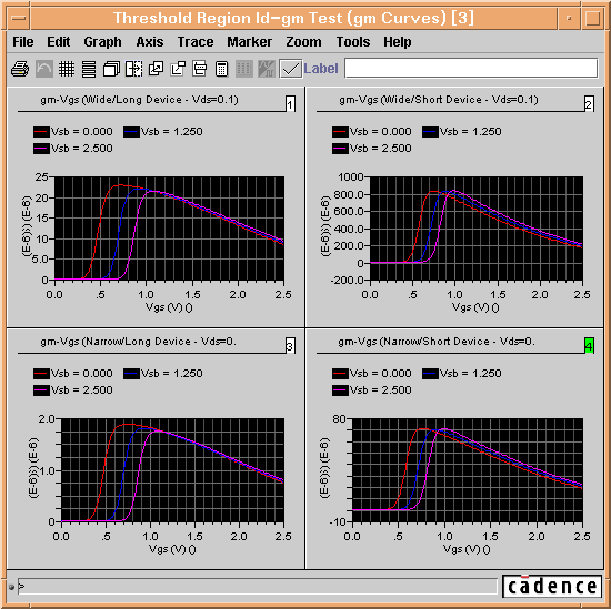
Vgs in threshold region, for
wide/long,
wide/short, narrow/long, and narrow/short devices. The playbacks are
for Vds=0.1 (5 Vsb
values) and Vgs swept from 0 to Vdd
in 0.02 V steps.
C.
Playbacks of Id
and gm versus
Vgs in subthreshold region, for wide/long, wide/short, narrow/long, and
narrow/short
devices. The playbacks are for Vds=Vdd (5 Vsb values)
and Vgs
swept from 0 to Vdd in 0.02
V steps.
2.
Tsividis-Suyama
tests
A.
Playbacks of Id,
gm, and gm/Id
versus Vgs in saturation
region, for wide/long,
wide/short, narrow/long, and narrow/short devices. The playbacks are
for Vds=Vdd and Vgs
swept from 0 to Vdd in 0.02
V steps.
B.
Playbacks of Id
and gd versus
Vds in saturation region, for
wide/long,
wide/short, narrow/long, and narrow/short devices. The playbacks are
for Vds=Vdd and Vgs
swept from 0 to Vdd in 0.02
V steps.
C.
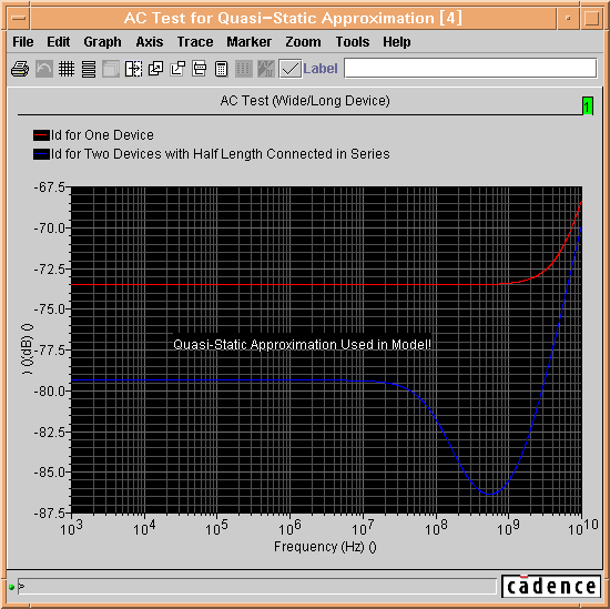
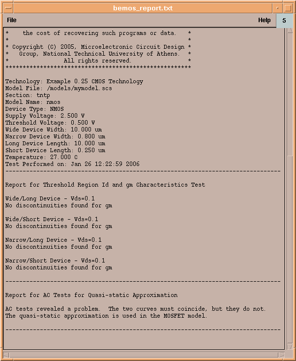
AC test to determine
whether or not the quasi-static
approximation is being used in the MOSFET model.
D.
Thermal noise test of
a device biased with a
fixed Vgs in strong
inversion and at Vds=0.
Under these conditions the channel is a resistor of value R=1/gd and
should show a thermal noise voltage with power spectral density of
4·K·T·R.
E.
Flicker noise test of
a device in strong
inversion saturation. The flicker noise should decrease 10x for a 10x
decrease
in channel width. It also should be insensitive in Vgs
changes.
3.
Isat tests
A.
Isat is plotted
over temperature.
B.
Isat is plotted
over channel length of the MOS device.
C.
Isat is plotted
over channel width of the MOS device.
4.
Fine grid
tests
A.
Playbacks of Id
and gm versus
Vgs in threshold region, for
wide/long,
wide/short, narrow/long, and narrow/short devices. The playbacks are
for Vds=0.1 (5 Vsb
values) and for 1000
values of Vgs swept from 0
to Vdd.
B.
Playbacks of Id
and gd versus Vds in saturation region, for wide/long and
wide/short devices. The playbacks are for Vsb=0
and Vsb=Vdd, Vgs=Vth-0.15,
Vth, Vth+0.15,
and 3 values of Vgs equally spaced between Vth and Vdd,
and for 1000 values of Vgs
swept from 0 to Vdd.
C.
This test is similar
to the test above, but is
done at one Vgs value over
a narrow range of Vds
values around saturation.
5.
Gummel tests
A.
Gummel
symmetry test.
B.
Slope
ratio test.
C.
Treetop
curve test.
6.
C-V characteristics
A.
Gate
capacitances (Cgs+Cgd,
Cgb, and Cgg=Cgs+Cgd+Cgb)
for wide/long, wide/short, narrow/long, and narrow/short devices, are
plotted over a fine Vgb grid
(0.01 V step from -Vdd
to Vdd) for Vds=0
and Vdd/2 and for Vsb=0
and Vdd.
B.
9
independent capacitance coefficients (Cgs, Cgd,
Cdg, Cbs, Cbd,
Cdb, Cgb, Csd,
Cbg) for wide/long,
wide/short, narrow/long, and narrow/short devices
are plotted over a fine Vdb
grid (0.01 V step from -Vth
to Vdd) for Vgs=Vdd (so operation is in
strong inversion) and Vsb=0.
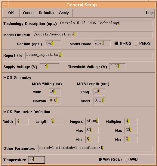
The form for setting up the necessary information for BEMOS is depicted below.
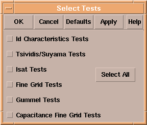
The form for selecting the tests is shown below.
Some example plots and a sample output report file are given below.
|
|
